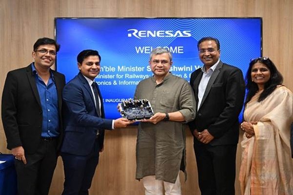
On 13 May 2025, Union Minister for Electronics and IT, Ashwini Vaishnaw, inaugurated state-of-the-art semiconductor design facilities in Noida and Bengaluru.
The key highlight is that this is India’s first design centre working on 3-nanometer chip design, placing the country in the global league of semiconductor innovation.
Mr. Vaishnaw called this a critical step toward building a nationwide semiconductor ecosystem, tapping into India’s vast engineering talent. The centre will allow end-to-end 3nm chip design within India—a national first.
He also launched a semiconductor learning kit to boost hands-on hardware skills among engineering students.
Over 270 academic institutions that already have EDA tools under the India Semiconductor Mission will now also get these new hardware kits.